KAGRA VIS Operations Manual - LVDT
LVDTs are used for vertical sensing and actuation in all the GAS filters and for horizontal sensing and actuation in all the IP stages.
See LVDT Signal Conditioning for useful background on LVDT demodulation.
See JGW-T1201255 for description of the Nikhef-supplied cards, and JGW-T1604798 for more information on how to tune the demodulation circuit.
LVDT Calibration Procedure: JGW-E1707287 or LVDT Calibration Procedure.
Type A
Your data here!
Type B Data
LVDT Drivers Data
For SR2:
LVDT Driver S.N. |
Left card |
Stage |
Resistor value [ohm] |
Reference Signal |
Gain |
Right card |
Stage |
Resistor value [ohm] |
Reference Signal |
Gain |
SR2: SN 7777777 |
R0 |
BF GAS |
59.2 |
4. Vpp |
4./5.02 = 0. |
R0 |
PI LVDT#1 |
50.1 |
4. Vpp |
4./5.02 = 0. |
R1 |
SF GAS |
36.3 |
4. Vpp |
4./5.02 = 0. |
R1 |
PI LVDT#2 |
50.6 |
4. Vpp |
4./5.02 = 0. |
|
R2 |
F0 GAS |
59.6 |
4. Vpp |
4./5.02 = 0. |
R2 |
PI LVDT#3 |
51.2 |
4. Vpp |
4./5.02 = 0. |
|
R3 |
Not used |
59.5 |
4. Vpp |
4./5.02 = 0. |
R3 |
Not used |
50.0 |
4. Vpp |
4./5.02 = 0. |
For SR3:
LVDT Driver S.N. |
Left card |
Stage |
Resistor value [ohm] |
Reference Signal |
Gain |
Right card |
Stage |
Resistor value [ohm] |
Reference Signal |
Gain |
SR3: SN 1807783 |
R0 |
BF GAS |
60.0 |
4.90 Vpp |
4.90/5.02 = 0.976 |
R0 |
PI LVDT#1 |
50.7 |
4.90Vpp |
4.90/5.02 = 0.976 |
R1 |
SF GAS |
60.7 |
4.86 Vpp |
4.86/5.02 = 0.968 |
R1 |
PI LVDT#2 |
50.7 |
4.88 Vpp |
4.88/5.02 = 0.972 |
|
R2 |
F0 GAS |
60.9 |
4.86 Vpp |
4.86/5.02 = 0.968 |
R2 |
PI LVDT#3 |
50.0 |
4.88 Vpp |
4.88/5.02 = 0.972 |
|
R3 |
Not used |
60.7 |
4.86 Vpp |
4.86/5.02 = 0.968 |
R3 |
Not used |
50.9 |
4.86 Vpp |
4.86/5.02 = 0.968 |
For SRM:
LVDT Driver S.N. |
Left card |
Stage |
Resistor value [ohm] |
Reference Signal |
Gain |
Right card |
Stage |
Resistor value [ohm] |
Reference Signal |
Gain |
SRM: SN 1807786 |
R0 |
BF GAS |
60.6 |
5.04 Vpp |
5.04/5.04 = 1.0 |
R0 |
PI LVDT#1 |
50.0 |
5.0 Vpp |
5.0/5.04 = 0.992 |
R1 |
SF GAS |
60.1 |
4.96 Vpp |
4.96/5.04 = 0.984 |
R1 |
PI LVDT#2 |
50.0 |
4.92 Vpp |
4.92/5.04 = 0.976 |
|
R2 |
F0 GAS |
60.7 |
4.96 Vpp |
4.96/5.04 = 0.984 |
R2 |
PI LVDT#3 |
50.5 |
4. Vpp |
5.0/5.04 = 0.992 |
|
R3 |
Not used |
61.2 |
4.94 Vpp |
4.94/5.04 = 0.98 |
R3 |
Not used |
50.8 |
4. Vpp |
4.9/5.04 = 0.972 |
New box for SRM. Adjusting the potentiometers to have the same values:
LVDT Driver S.N. |
Left card |
Stage |
Resistor value [ohm] |
Reference Signal |
Gain |
Right card |
Stage |
Resistor value [ohm] |
Reference Signal |
Gain |
SRM: SN 1403020 |
R0 |
BF GAS |
60.2 |
- Vpp |
- = - |
R0 |
PI LVDT#1 |
50.4 |
- Vpp |
- = - |
R1 |
SF GAS |
60.1 |
- Vpp |
- = - |
R1 |
PI LVDT#2 |
50.3 |
- Vpp |
- = - |
|
R2 |
F0 GAS |
60.7 |
- Vpp |
- = - |
R2 |
PI LVDT#3 |
50.3 |
- Vpp |
- = - |
|
R3 |
Not used |
61.0 |
- Vpp |
- = - |
R3 |
Not used |
50.2 |
- Vpp |
- = - |
Yoke Height Settings
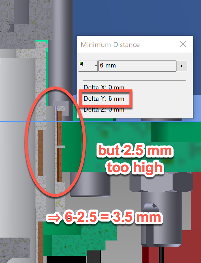
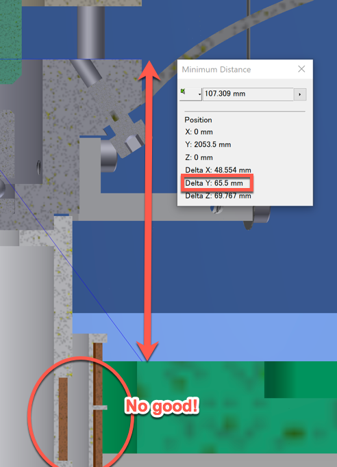
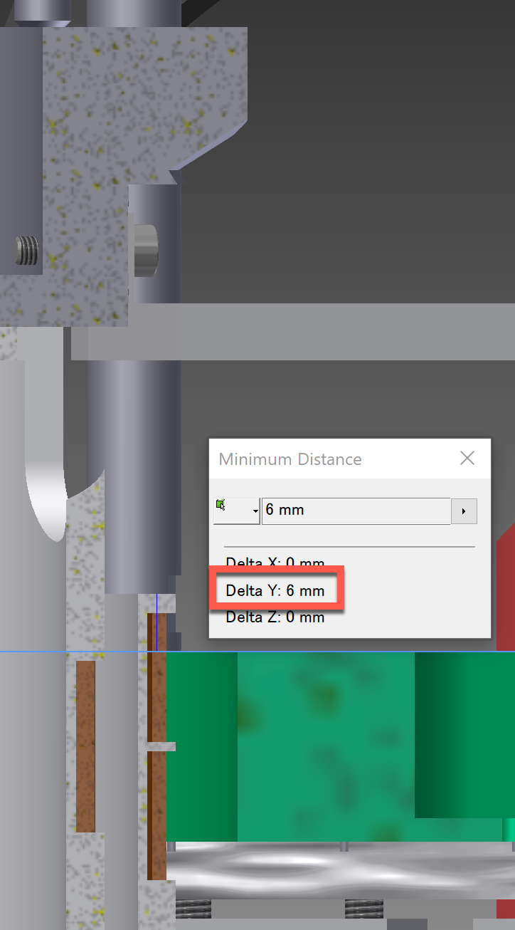
The yoke should be set so that the double and single LVDT coils are symmetrically aligned when the keystone is at nominal height. It is convenient to set this in terms of the amount the PEEK coil former sticks out above the filter baseplate.
Bottom Filter (BS and SRx)
Note that the CAD is wrong for the bottom filter yoke:


Standard Filter (BS and SRx)

Top Filter (BS and SRx)
Summary
GAS Filter |
Yoke Height |
Keystone Height |
BS BF |
3.5 mm |
65.5 mm (up from baseplate) |
SR BF |
3.5 mm |
65.5 mm (up from baseplate) |
BS SF |
6 mm |
65.5 mm (up from baseplate) |
SR SF |
6 mm |
65.5 mm (up from baseplate) |
BS F0 |
36 mm |
153 mm (up from top plate), 16.5 mm (down from ring) |
SR F0 |
34 mm |
153 mm (up from top plate), 16.5 mm (down from ring) |
Type Bp Data
Your data here!
Stocktake
LVDT Stocktake as at 2018-04-13
See JGW-D1402826-v2: LVDT Driver Module Top Assembly.
* = sighted recently
Faulty (3)
- S1807786*: 2018-04-11 Found to be faulty - returned to Mozumi by Enzo
- S1807785*: Failed during measurement 2019/2/20
- S1403130: Both of them are in a bad condition. The S number of the Input LVDT Card is shown below. // S1403106 // S1403161 // (2017/07/21 AEL)
In use, presumably OK (14)
- S1807787: 2018/4/4: Moved to NAOJ for TMS by Miyakawa, Akutsu
- S1807783: 2018-03-12 Moved to SR3 rack area for SR3/SRM by Mark, Enzo
- S1807784: Installed to IXV. 2018/2/14
- S1403137: [2017/09/29] Installed into K1EX2 rack by K. Okutomi
- S1403049: [2017/07/25] Installed into K1EX2 rack by K. Okutomi
- S1403048: Installed into EY2 rack by K. Okutomi, June 9, 2017 // We replaced the front panel with that of Ver. 2.(EY1 Rack) 2017/07/13 AEL
- S1403047: Moved to PR2 rack (June 2017) // We replaced the front panel with that of Ver. 2.(PR2 Rack) 2017/07/06 AEL
- S1403133: Installed for PR3 BF LVDTs (Feb 2017) // We replaced the front panel with that of Ver. 2.(PR0 Rack) 2017/07/06 AEL
- S1403046: We replaced the front panel with that of Ver. 2.(EY1 Rack) 2017/07/13 AEL
- S1403131: We replaced the front panel with that of Ver. 2.(PR0 Rack) 2017/07/06 AEL
- S1403050: We replaced the front panel with that of Ver. 2.(PR2 Rack) 2017/07/06 AEL
- S1403044: 2017-11-16 SR3 rack was reassigned as SR2 by Mark, Miyakawa. Chassis was confirmed to be inside.
- S1403052: Brought into the tunnel (PR3) on November 19, 2015 // We replaced the front panel with that of Ver. 2.(BS Rack) 2017/07/06 AEL ????
- S1403136: We replaced the front panel with that of Ver. 2.(PR0 Rack) 2017/07/06 AEL
In use, needs new front panel (1)
- S1403020: 2018-04-12 Installed in SRM to replace faulty 7786 by Enzo. (Still has old-style panel.)
In circuit room (11)
- S1403132*: We replaced the front panel with that of Ver. 2. 2017/07/10 AEL (Keep in circuit room after replacement)
- S1403134*: We replaced the front panel with that of Ver. 2. (2017/07/27 AEL)
- S1403051*: We replaced the front panel with that of Ver. 2. 2017/07/10 AEL
- S1403045: We replaced the front panel with that of Ver. 2. 2017/07/10 AEL
- S1403139*: We replaced the front panel with that of Ver. 2. 2017/07/10 AEL
- S1403138*: We replaced the front panel with that of Ver. 2. 2017/07/10 AEL
- S1807792: Assembled in Kamioka (OSC circuit is not installed). 2018/2/9
- S1807791: Assembled in Kamioka (OSC circuit is not installed). 2018/2/9
- S1807790: Assembled in Kamioka (OSC circuit is not installed). 2018/2/9
- S1807789: Assembled in Kamioka (OSC circuit is not installed). 2018/2/9
- S1807788: Assembled in Kamioka (OSC circuit is not installed). 2018/2/9
In circuit room, needs new front panel (1)
- S1403135: It needs to be replaced with a panel of Ver. 2.(2017/07/18 AEL)
